

A new epitaxial mechanism enables ultra-high quality Ag films on Cu substrates

It is straightforward to produce polycrystalline metal films on wafers but producing single‑crystal metal films is far more challenging. Because single crystals have no grain boundaries (the joints between differently oriented crystal regions in polycrystalline materials), they offer much better electrical performance: higher conductivity, lower resistive losses, improved high‑frequency behaviour (important for high‑speed communication and 5G), and reduced noise for quantum technologies. As a result, methods for reliably producing single‑crystal films are highly sought after.
Single‑crystal silver and copper films are particularly valuable. Silver is an exceptional conductor of both electricity and light, while copper provides excellent thermal management and reduces resistive heating. However, growing silver on copper is notoriously difficult because the two materials have a large lattice mismatch (13%), which normally introduces strain, defects, dislocations, and rough, low‑quality films. This makes conventional epitaxy essentially impossible.
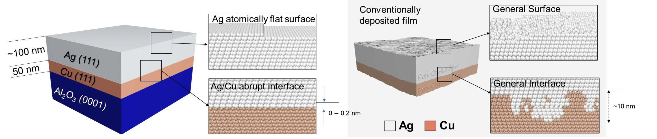
In this work, the researchers overcame this barrier using Atomic Sputtering Epitaxy, which allows precise atomic deposition, combined with post‑annealing to reduce twin boundaries. They discovered that the mismatch strain is absorbed entirely within the first atomic layer of silver. This occurs because the atoms at the interface shift sideways in a periodic, controlled pattern that releases the strain. This represents a new form of heteroepitaxy in which two materials with different lattice periodicities can still grow together seamlessly.
They demonstrated wafer‑scale, defect‑free single‑crystal silver films on copper despite the huge lattice mismatch, enabling ultra‑high quality metal films for advanced optical and electronic technologies. This approach opens the door to new heteroepitaxial systems and provides a route to producing silver films with exceptional optical and electronic performance.
“What we find most notable is that a 13% lattice mismatch, which would normally prevent clean heteroepitaxy, is absorbed almost entirely within the first monoatomic Ag layer at the Ag/Cu interface, allowing the film above to grow as if on its own native lattice and yielding wafer-scale, grain-boundary-free films with atomically flat surfaces. We hope this concept of a strain-absorbing monolayer interface can be extended to other dissimilar metal pairs.” – Professor Young-Min Kim, Sungkyunkwan University
Do you want to learn more about this topic?
Si/Ge nanostructures by Karl Brunner (2001)


